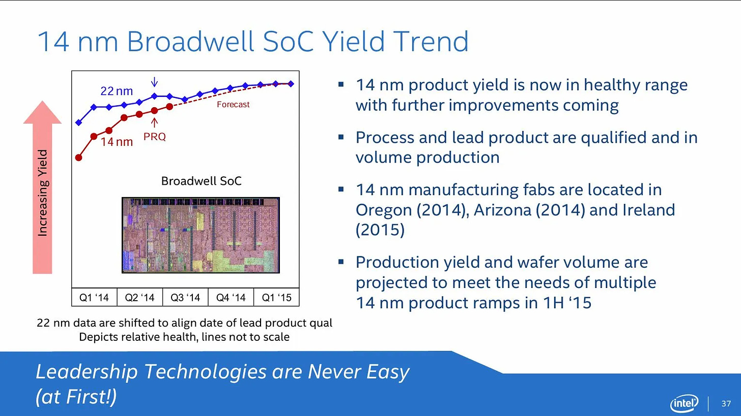
Up to Haswell’s 2013 release, Intel’s “tick-tock” strategy seemed unstoppable. Broadwell sought to continue Intel’s juggernaut by porting Haswell to a new 14 nm node. The new node would lower power consumption, while minor architecture changes targeted a 5% IPC increase. Intel had good reason to believe everything would go according to plan. Tick-tock had gone well for the past few generations, and Broadwell’s minor architecture changes would let engineers focus on any process node issues. Unfortunately, 14 nm node issues proved to be too much. Broadwell did well in mobile and server chips, environments that favor low per-core power consumption. But Intel’s flagship desktop chips continued to use Haswell. Broadwell could not match Haswell’s clock speed, and the minor IPC boost did not compensate.
However, Broadwell’s limited desktop release is particularly interesting because it came with 128 MB of eDRAM based L4 cache. Broadwell couldn’t act as a high performance desktop flagship, but Intel took the opportunity to shake things up and go for high iGPU performance. Large iGPUs demand a lot of bandwidth, and the L4 cache aimed to enable high iGPU performance on a standard dual channel DDR3 setup. Even better, the L4 could serve the CPU cores too. That meant Intel had a large last level cache on a desktop CPU, nearly seven years before AMD launched the Ryzen 7 5800X3D with vertically stacked cache to give 96 MB of L3.
Special thanks goes to Crispysilicon for making a Xeon E3-1285 v4 available for testing. I’d also like to thank cha0shacker for providing data from Broadwell and Skylake eDRAM configurations.
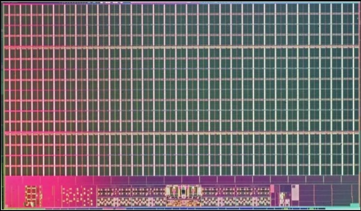
Broadwell implemented its L4 cache on a separate 77mm2 die, creating a chiplet configuration. This cache die was codenamed “Crystal Well”, and was fabricated using the older 22nm process. Crystal Well actually made its first appearance during the Haswell generation, where it demonstrated enough potential for Intel to carry it forward. As on Haswell, Crystal Well connects to Broadwell’s CPU die via an OPIO (On-Package IO) interface.
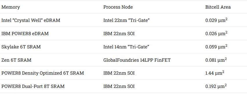
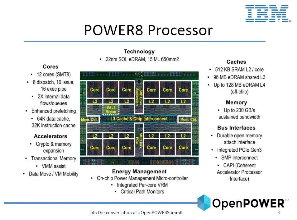
Memory arrays on the cache die use eDRAM, or embedded Dynamic Random Access Memory. Cache typically uses static RAM (SRAM), which uses several transistors to store a single bit. A DRAM bit only needs a transistor and a capacitor, providing improved density. While DRAM is more often used for main system memory, Intel is far from the only manufacturer to use eDRAM. IBM was doing the same for POWER’s L3 caches.
Both 22nm eDRAM implementations exhibit excellent storage density, even compared to SRAM cells on newer 14 nm nodes. However, DRAM is quite a troublesome technology to work with if you want high performance at low power. Capacitors will slowly lose their charge, so DRAM must be periodically refreshed to maintain data integrity. Reads require draining each DRAM cell capacitor’s charge, so DRAM cells need time to recover as supporting logic puts charge back after a read. But as with many technologies, there’s plenty of room in DRAM design to make cost, density, power, and performance tradeoffs. Unlike DRAM modules used for main memory, Intel designed the eDRAM chip for high performance at low power. It therefore has some nifty features, even if it can’t approach SRAM’s power efficiency and speed.
For starters, Crystal Well has a massive 128 banks compared to DDR3’s eight or even DDR5’s 32. Dividing the DRAM array into banks gets around the destructive read problem because the read+recovery process happens independently for each bank. Higher bank count decreases the chance of an incoming access clashing into a still-recovering bank.
Besides more banks, Crystal Well’s banks recover in just six array cycles. For comparison, bank random cycle time on main memory DDR is often dozens of cycles. More banks and better banks translate to more consistent random access performance, especially under high bandwidth load.
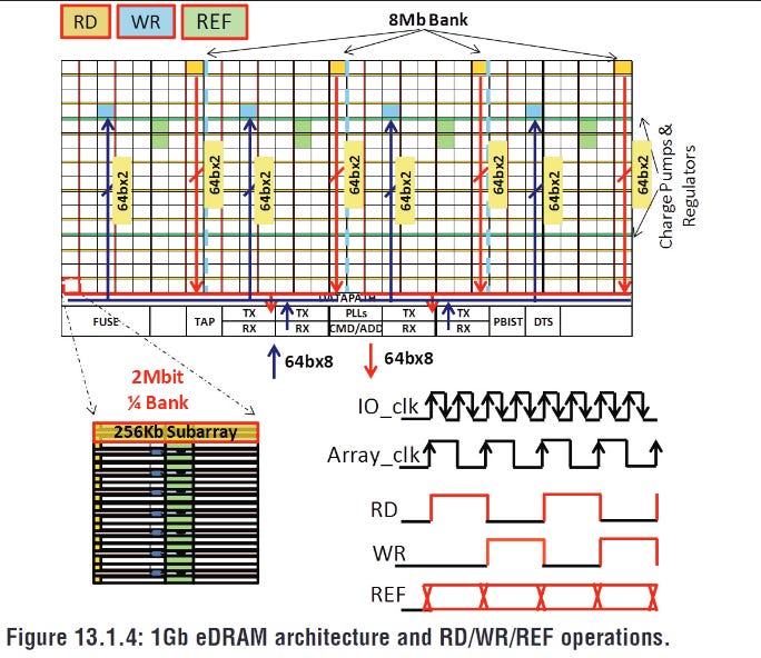
Crystal Well’s OPIO interface is also built to deliver more consistent performance. It has separate 64-bit read and write buses, while standard DDR uses a single set of pins for both reads and writes. DDR memory controllers have to do bus “turnarounds” to switch between read and write mode. Turnarounds take time, leaving the bus unused until it can complete. That creates a nasty scheduling problem when handling mixed read and write traffic. Separate read and write buses mean Crystal Well doesn’t need to do bus turnarounds, and can even service reads and writes on alternating cycles. The OPIO interface only has one address bus, but that’s enough to saturate the data buses. Each access is for a 64B cacheline (512 bits), and reading out 64 bytes takes two cycles. Alternating read and write requests will actually maximize bandwidth by using both directions on the data bus.
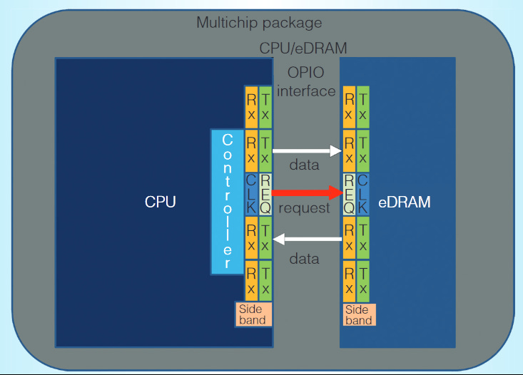
DRAM’s refresh problem also gets tackled by Crystal Well’s high bank count, because Crystal Well can independently refresh 64 bank-groups, each consisting of two banks. Banks not being refreshed remain free to serve accesses. In contrast, standard DDR3 has to refresh all banks in a rank together. DDR3L and LPDDR3 can do per-bank refresh, but still have fewer banks compared to Crystal Well, increasing the chance of a request clashing into a bank busy getting refreshed.
For power savings, Crystal Well can enter a self-refresh mode where it powers off the OPIO interface and handles data retention autonomously. Standard DDR for comparison always needs the memory controller to issue refresh commands.
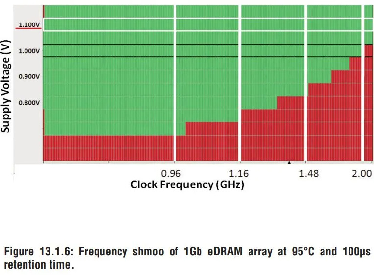
Finally, Crystal Well goes fast. A 1.6 GHz eDRAM clock and double-clocked OPIO interface make Crystal Well the equivalent of DDR-3200, with timings main memory DDR can only dream of. DDR3-1866 is already quite fast for Broadwell’s time, and DDR4-3200 would not be common until several years later. Technically, Crystal Well can run up to 2 GHz, providing 64 GB/s of theoretical bandwidth in each direction with even better latency. All this can be accomplished with under 1.1V of voltage, compared to the 1.5V used by standard DDR3. As for power, Intel claims the OPIO interface only consumes 1W of total power to deliver 102 GB/s (3.2 GHz clock, both directions in use).
Of course all this comes at a cost. Each bank needs independent logic to handle addressing and recovery from destructive reads. Self-refresh logic means even more supporting logic. Die space used for logic is of course die space not used for DRAM bitcells. Beyond the die, read and write buses mean more PCB traces. Thus Crystal Well can’t provide enough capacity to function as main memory, and can’t provide flexible capacity the way removable DIMMs can. But its speed and power efficiency lets it work as a L4 cache.
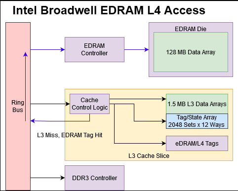
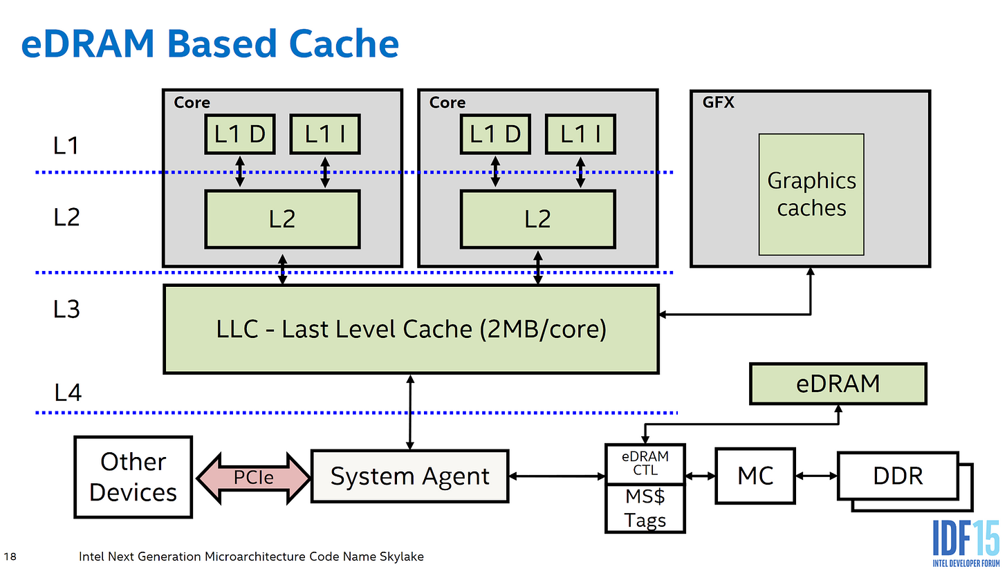
On Haswell and presumably Broadwell, Crystal Well acts as a non-inclusive victim cache. That means it’s filled by “victim” lines kicked out of L3 to make room for fresher data. Non-inclusive means the eDRAM doesn’t have to hold data already held in upper level caches. The Crystal Well die only contains eDRAM data arrays and simple control logic. Intel needs extra storage and tags to make the eDRAM work as a cache, and that goes into Broadwell’s L3 slices.
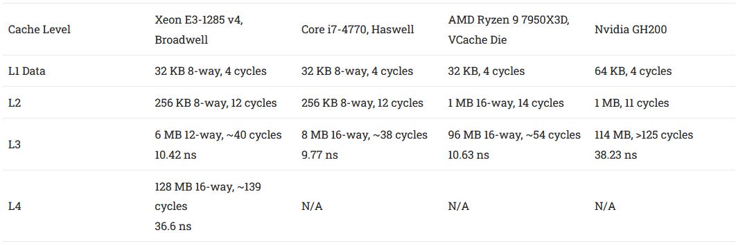
Caches need tags to track what they’re caching, much like how supermarket tags track what products are on shelves. Broadwell’s L3 cache shrinks from 8 to 6 MB to make room for those tags. Putting L4 tags on the CPU die makes sense because tags have to be checked with each access. A set associative cache requires tag checks for each way, so tags see a lot of traffic and must deliver high performance at low power. Implementing tags on the CPU die lets Intel use SRAM on a leading edge process node, which is well suited to the task.
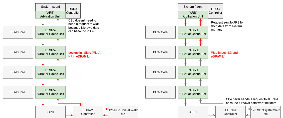
eDRAM tags are checked in parallel with L3 tags, so L3 cache control logic also handles L4 caching. That way, L4 misses don’t require an extra trip on the ring bus to get to system memory.
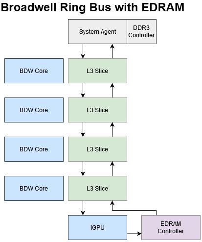
Intel’s L4 setup for Broadwell and Haswell is well thought out to minimize latency both for L4 hits and misses.
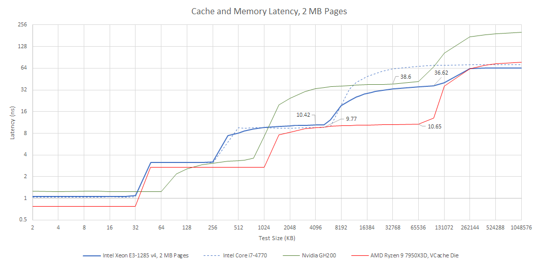
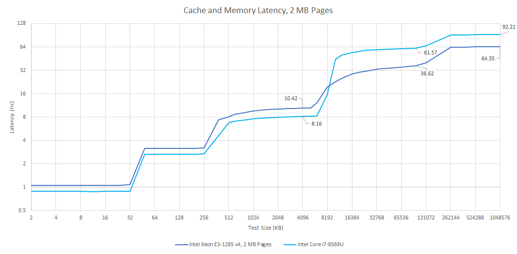
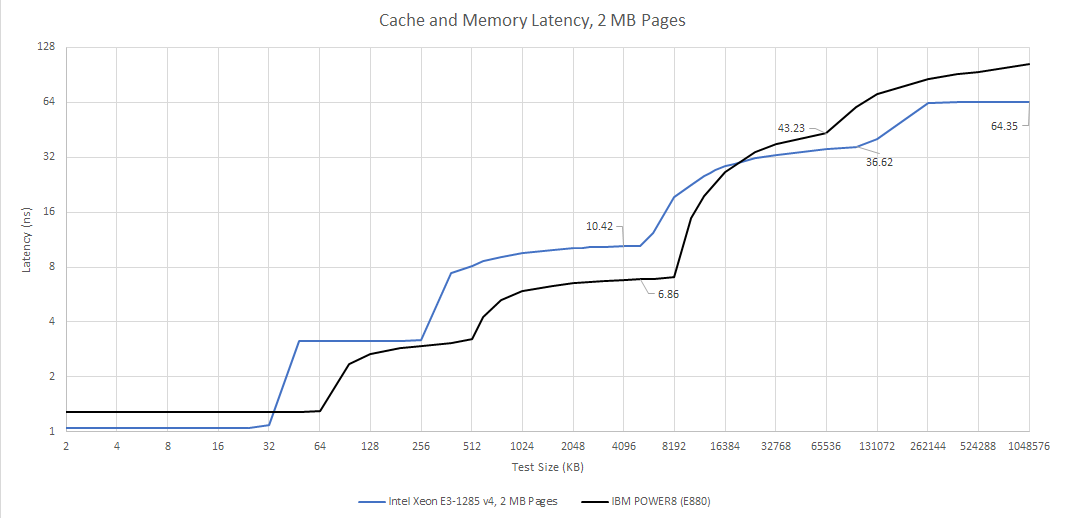
L4 accesses have about 36.6 ns of load-to-use latency, or nearly 140 cycles at 3.8 GHz. eDRAM isn’t a good L3 solution, so Broadwell’s 6 MB L3 still plays an important role. Slower L3 caches do exist if you look hard enough, but I think such slow L3 caches are non-ideal.
Against a last generation Haswell chip without eDRAM, Broadwell with eDRAM enjoys much better latency as data footprints spill out of L3. Thanks to Broadwell’s latency focused design, main memory latency remains excellent. In fact, the Broadwell system Crispysilicon set up had just 64.3 ns of load-to-use DRM latency at the 1 GB test size. Haswell got 71.2 ns of latency at the same test size. But that has more to do with the Broadwell system getting fast DDR3-1866 11-11-11. I had my Haswell system set up with spare DDR3-1333 CL9.
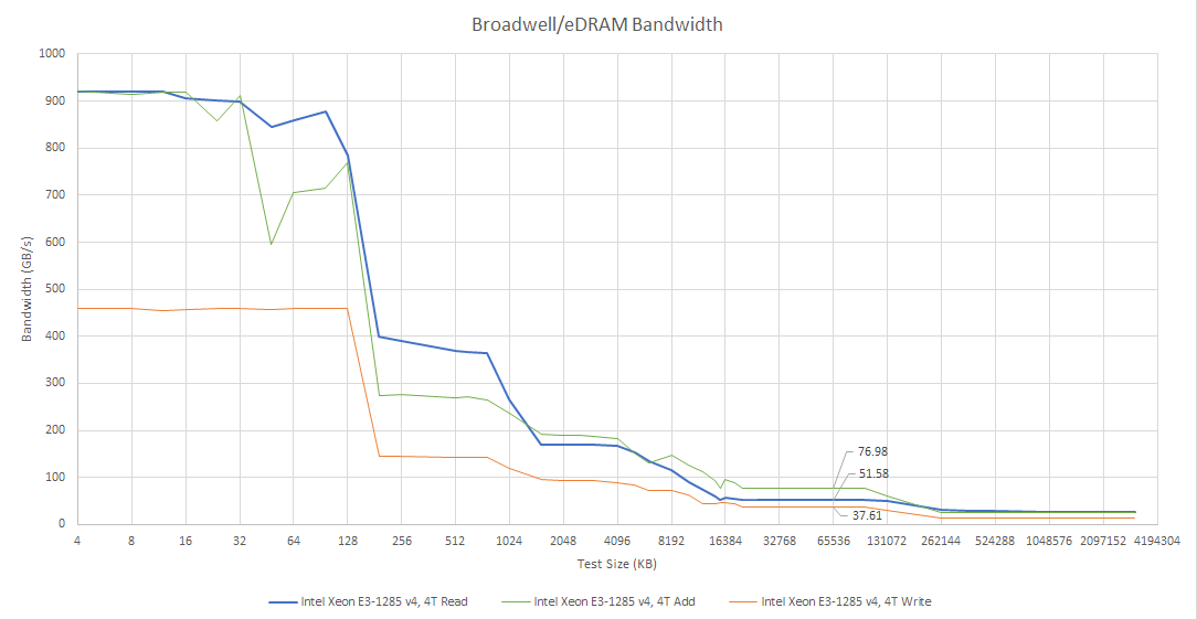
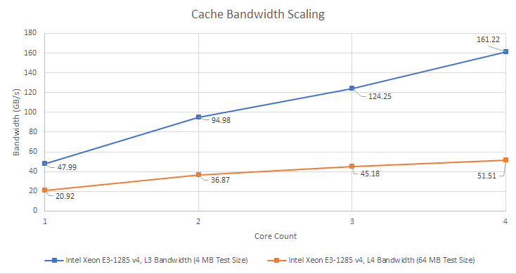
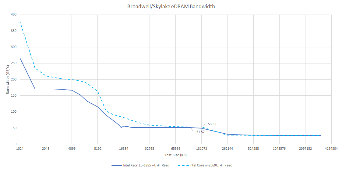
eDRAM bandwidth is limited by the OPIO interface, and maxes out at just over 50 GB/s. Bandwidth is somewhat higher if I use a read-modify-write pattern, which generates read and write traffic in equal proportions. But it isn’t quite doubled compared to read-only bandwidth. Perhaps I’m hitting bank conflicts with such high bandwidth load.
Unlike Broadwell’s L3 cache, eDRAM bandwidth can’t scale with core count. That’s a problem because even a quad core CPU has no problem saturating the OPIO interface. eDRAM only has a single OPIO interface, over which it can deliver 32 bytes per cycle at array clock. In contrast Broadwell’s L3 is split into slices, with slice count equal to core count. Each L3 slice can deliver 32 bytes per cycle at uncore clock, which is typically much higher than eDRAM clock. Multiple L3 slices let L3 cache bandwidth scale with core count. Even if Intel were able to clock the eDRAM and OPIO interface higher, it would eventually run into the bandwidth limitations of a single ring stop.
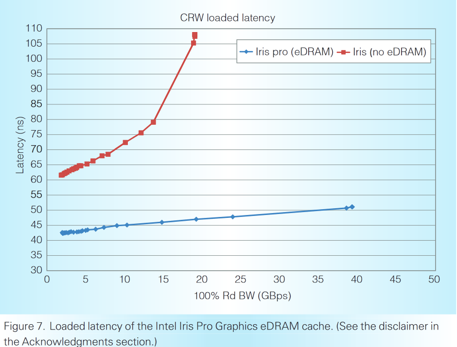
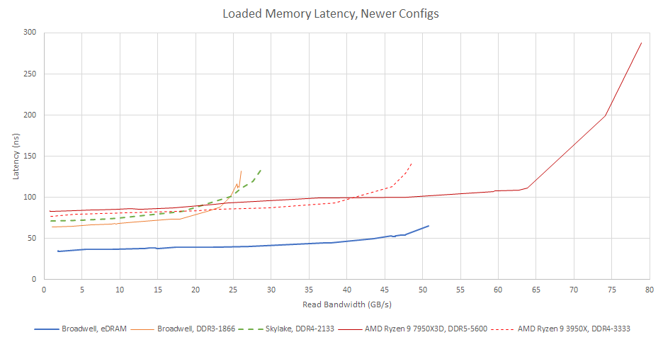
Latency and bandwidth can be closely related in practice. Average request latency can sharply increase as a workload approaches bandwidth limits, because requests start queuing up waiting to use the memory bus. Intel notes their eDRAM is optimized for low latency, and suffers minimal latency penalties as bandwidth demands increase.
eDRAM is also carefully designed to minimize latency, as the outstandingly small latency sensitivity with load sustainable for random traffic shown in Figure 8, which is especially important for eDRAM to benefit not only graphics but also general CPU workloads
Haswell: The Fourth-Generation Intel Core Processor
High bank count, separate read/write buses, and fast bank cycle time likely all contribute to improving average latency under high load. More bandwidth of course improves latency too, as latency is more likely to remain low as applications demand more bandwidth. Intel tested Haswell parts both with and without eDRAM, and saw eDRAM behave far better under high load.
I don’t have a directly comparable non-eDRAM part, so I’m replicating this test on Broadwell by sizing latency/bandwidth tests to fit either in eDRAM or spill into main memory. I spawn a variable number of bandwidth test threads, which can optionally throttle themselves by busy-looping with each loop iteration. I also spawn a latency test thread pinned to a separate core. The latency test thread allocates memory with 2 MB pages to reduce address translation overhead.
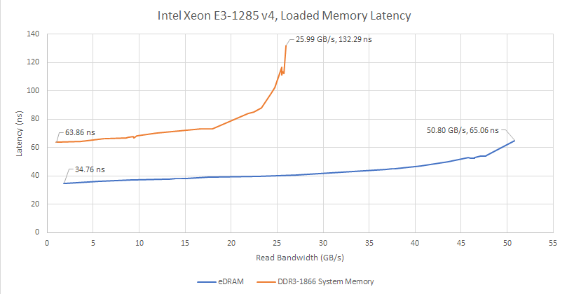
I suspect Intel used 4K pages, so address translation latency slightly increased their total latency figures. Page walks could further consume cache and memory bandwidth. Still, I can broadly replicate Intel’s results by testing on Broadwell. eDRAM sees a very gentle latency rise as I push toward its bandwidth limits. I can even achieve 99% bandwidth efficiency, though doing so almost doubles latency compared to the best case scenario. Main memory DRAM fares far worse, with latency passing 101 ns as I pass 85% bandwidth utilization.
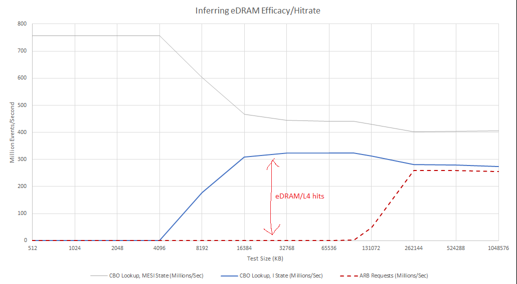
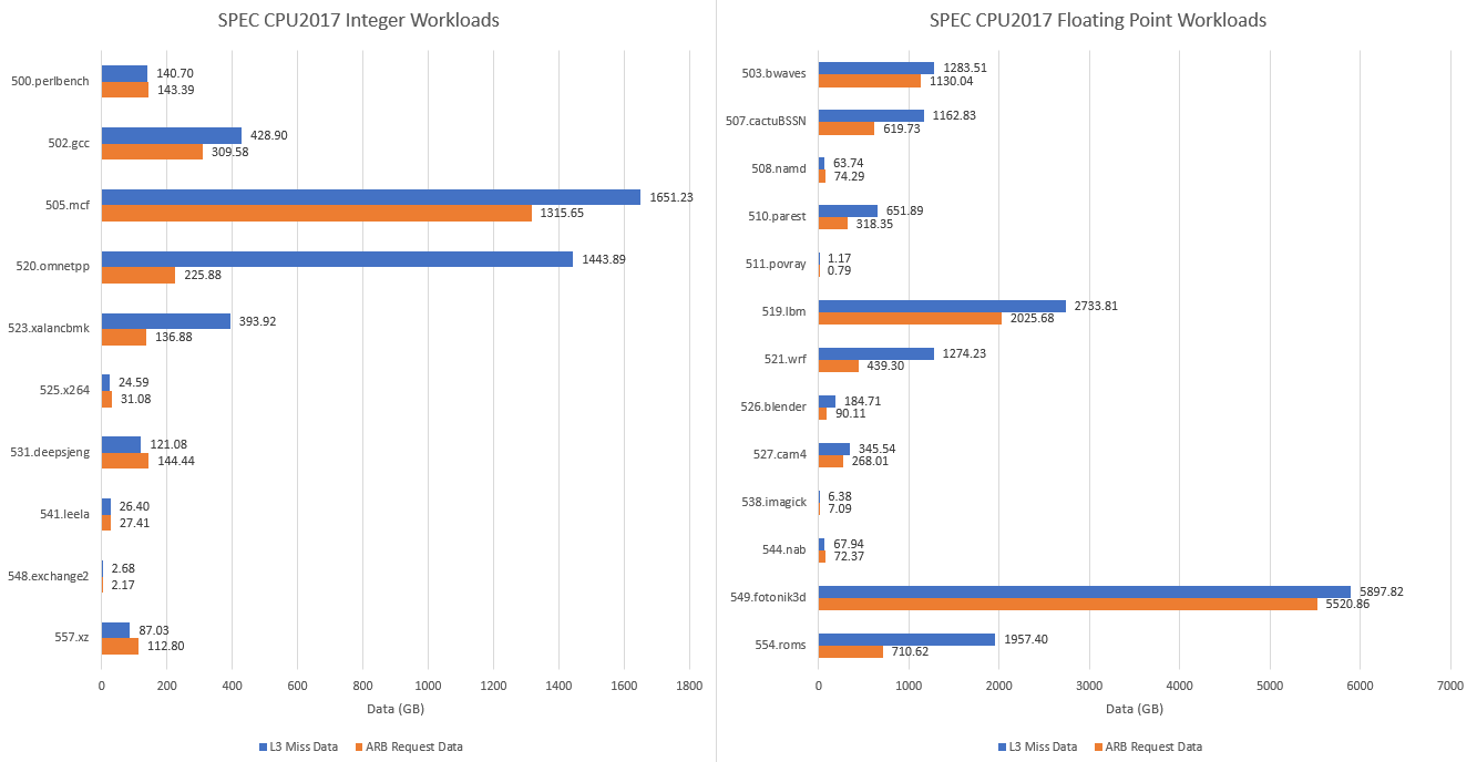
Intel did not publish any eDRAM-related performance monitoring events for Broadwell. I went about trying to infer eDRAM efficacy using other metrics. One attempt involved looking at CBo and ARB counters. CBo, or Cache Box, is Intel’s name for L3 cache slices. Each CBo has a couple of counters that support lookup state events. A lookup in I (invalid) state indicates a L3 miss.
ARB is the arbitration unit at the System Agent. The System Agent sits on the ring bus and acts as a bridge for the iGPU and CPU cores to access memory and IO. In addition, the System Agent contains a power control unit and display engine. The arbitration unit has a queue that sits between the ring bus and rest of the System Agent, and is responsible for tracking requests from the cores or iGPU.
Without eDRAM, a L3 miss would usually have to be satisfied from DRAM, which involves sending a request to the ARB queue. However an eDRAM hit doesn’t need to involve ARB, because the CBo can obviously satisfy it from eDRAM. I ran my memory bandwidth test at various sizes while checking CBo/ARB events to see whether this method could work.
However, counter values from a full SPEC run were more difficult to interpret. Evidently, a L3 miss can result in more than one ARB request. For example, a L3 miss gets satisfied by an ARB request. It could replace a line in L3 (a victim), which gets copied to eDRAM. That in turn replaces a line in eDRAM. If that eDRAM victim is modified, it must be written back to main memory, causing another ARB request. That’s a far from satisfactory explanation though, because I see ARB requests slightly outnumber L3 misses on my eDRAM-less Core i5-6600K. Something else is going on that I don’t understand.
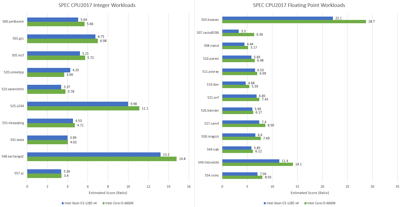
Still, the data suggests eDRAM makes a noticeable difference in a few SPEC CPU2017 workloads. 520.omnetpp is a particularly interesting example. It sees a lot of L3 miss traffic, and over 84% estimated L4 hitrate is enough to let Broadwell beat the higher clocked and newer Skylake architecture.
But Broadwell is unable to win in any other tests. Skylake’s better architecture and the Core i5-6600K’s slightly better clock speed (3.9 vs 3.8 GHz) carry the day.
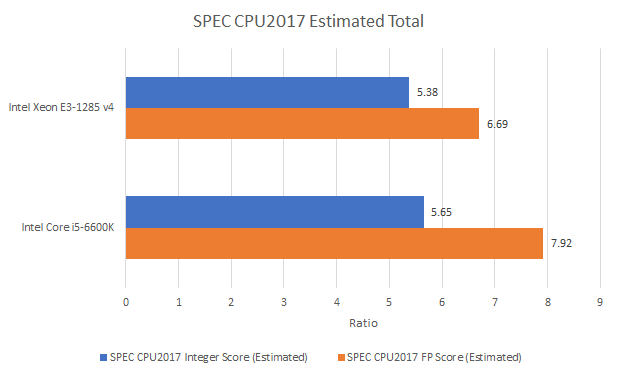
In retrospect, I can understand why Broadwell’s desktop release was so limited. eDRAM doesn’t provide a consistent enough performance advantage, and Skylake was less than a year away. Including a 77mm2 eDRAM die is sure to increase costs too. Overall, Skylake leads Broadwell by 5% in the SPEC CPU2017 integer suite, and 18.3% in the floating point suite.
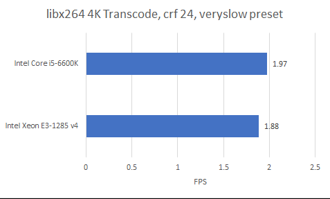
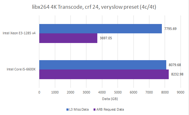
SPEC CPU2017 features a wide variety of workloads. But because it’s meant to test the compiler as well as hardware, it doesn’t have hand-optimized assembly. That leaves a gap, hand-optimized assembly is used when performance is an important enough consideration. Software video encoding is one of those applications. It offers better space and quality tradeoffs than hardware encoders, but does so by being more computationally expensive. libx264 has assembly optimized paths for just about every popular ISA, making it a convenient test. Here, I’m running the workload pinned to one thread of each physical core.
In this vector heavy test, Skylake leads Broadwell by 4.8%. But performance counters indicate eDRAM cuts System Agent traffic by more than half. That implies DRAM traffic is roughly halved too.
eDRAM’s ability to reduce main memory traffic could come in handy for a memory bandwidth constrained platform, like a hypothetical setup with first generation DDR3. But for a Core i5-6600K with dual channel DDR4-2133, DRAM bandwidth is rarely a concern. As memory technology continued to advance, Crystal Well’s advantage steadily diminished.
Intel continued to use Crystal Well on certain Skylake SKUs, but revised the system architecture to put eDRAM-related logic in the System Agent. eDRAM tags move off the L3 and into the System Agent, and the eDRAM controller no longer gets its own ring stop.
All main memory accesses can benefit from eDRAM caching with this revised setup. Intel’s display engine is one notable beneficiary, because keeping a screen refreshed can account for a surprising amount of data transferred from DRAM. For a laptop where a user might be reading a webpage or editing a document, the display engine can be a major consumer of DRAM bandwidth while the CPU cores are mostly idle.
Like Broadwell, Skylake’s eDRAM can provide more bandwidth than system memory. Bandwidth seems to have improved slightly, so Intel may have slightly increased eDRAM and OPIO clocks.
In exchange for reducing main memory traffic though, Intel ditched Broadwell’s latency optimized setup. eDRAM tags are no longer checked alongside L3 accesses. Thus the CPU doesn’t know whether it can get data from eDRAM until a L3 miss request arrives at the System Agent and eDRAM tag checks finish. Accessing eDRAM tags in parallel with main memory would defeat the point of eDRAM, main memory access can only start once eDRAM tag checks finish and determine a L4 miss. That’s something Broadwell sought to avoid.
Skylake basically moves the eDRAM L4 cache farther away from CPU and iGPU cores, and closer to the memory controller. CPUs are more latency sensitive than the iGPU or display engine, which means CPU performance gets the short end of the stick. Skylake’s eDRAM load-to-use latency approaches that of fast DDR3. Main memory latency regresses, hurting workloads that aren’t cache friendly.
And while eDRAM bandwidth remained unchanged, main memory technologies steadily advanced. Later DDR4 generations can get very close to eDRAM bandwidth, though of course not with the same low latency.
With DDR5, main memory can surpass eDRAM bandwidth while keeping latency under control as bandwidth demand pushes past 50 GB/s. The OPIO interface is totally out of date. And in fairness to Intel, consumer on-package PCB traces haven’t gotten much faster. AMD’s on-package Infinity Fabric (IFOP) links on Zen 2 and later only deal with DRAM and IO traffic. They simply don’t have enough bandwidth to service a cache.
Crystal Well is an example of DRAM tuned for performance, rather than high capacity at low cost. Main memory DRAM loses performance because of a unidirectional bus, low bank count, and high bank cycle time. All of those are design choices meant to simplify DRAM chips, not inherent limitations of DRAM technology. If engineers design DRAM and the supporting system architecture to do so, eDRAM can provide better density than SRAM while delivering better performance than main memory DRAM.
IBM’s POWER8 eDRAM is another good example. IBM accesses its eDRAM within a monolithic die, using it to implement L3 cache. eDRAM load-to-use latency in that platform is 6.86 ns, fast even by L3 cache standards. It’s a demonstration of just how fast DRAM can go when supported by a system architecture that lets it shine.
With POWER8 in mind, even Broadwell’s system architecture makes a compromise between cost and performance. OPIO uses plain on-package traces instead of a costly embedded bridge or interposer. eDRAM was not implemented on a leading edge node. And Broadwell uses a chiplet design to implement a L4 cache, not a large monolithic die.
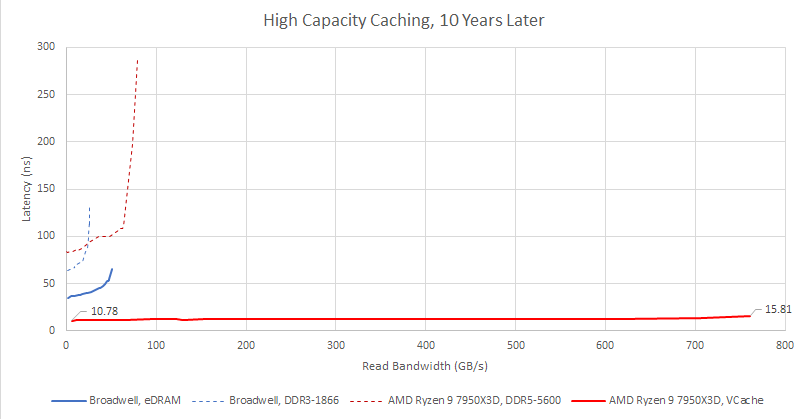
I’m fascinated by what eDRAM was able to achieve. But SRAM density has gone up with each process node generation, enabling higher capacity caches without DRAM difficulties. AMD’s VCache is a spiritual successor to Broadwell’s eDRAM. Both solutions add a cache die to give CPU cores massive caching capacity. However, AMD links the cache die with advanced packaging technology, and uses higher performance SRAM. It’s a solution tightly optimized for improving CPU performance. Unsurprisingly, VCache’s performance characteristics are worlds ahead of Crystal Well’s.
Intel also took advantage of SRAM density scaling. Even though Intel didn’t use SRAM to the same extent as AMD, recent Intel parts have far more caching capacity than their Broadwell ancestors. Meteor Lake’s iGPU has 4 MB of L2 cache, giving it four times as much private cache as Broadwell’s iGPU. The CPU side has 24 MB of L3, also 4x as much as Broadwell’s CPU. My Meteor Lake laptop has a LPDDR5-7467 setup with over 100 GB/s of theoretical bandwidth on tap – so much that I can’t saturate the LPDDR5 bus with just CPU cores.
With bigger SRAM-based caches and more memory bandwidth, Intel too no longer saw the need for a large L4 cache. Even if Intel advanced eDRAM technology, a Broadwell-like strategy would likely face difficulties with cheap on-package traces. But I wonder if Intel could pull off high capacity caching sometime in the future. AMD VCache chips offer competitive gaming performance with excellent power efficiency. Intel has their own advanced packaging technologies, with vertical stacking and a base die without active logic. That’s not to say adding a high capacity cache would be easy. But I think high capacity caching is a fun part of Intel’s history. It would be fun to see it return.
If you like our articles and journalism, and you want to support us in our endeavors, then consider heading over to our Patreon or our PayPal if you want to toss a few bucks our way. If you would like to talk with the Chips and Cheese staff and the people behind the scenes, then consider joining our Discord.
-
Fatih Hamzaoglu et al, A 1 Gb 2 GHz Embedded DRAM in 22nm Tri-Gate CMOS Techhnology, ISSCC 2014
-
Teja Singh et al, Zen: An Energy-Efficient High-Performance x86 Core, IEEE Journal of Solid State Circuits 2018
-
Eric J. Fluhr et al, POWER8: A 12-Core Server-Class Processor in 22nm SOI with 7.6Tb/s Off-Chip Bandwidth
-
Per Hammarlund et al, Haswell: The Fourth-Generation Intel Core Processor, IEEE 2014
-
Jonathan Chang et al, A 7nm 256Mb SRAM in High-K Metal-Gate FinFET Technology with Write-Assist Circuitry for Low-Vmin Applications, ISSCC 2017
-
Only DDR3L can do per-bank refresh: https://onlinedocs.microchip.com/oxy/GUID-BCEA4067-D69A-4529-81CC-133D9195C03C-en-US-4/GUID-8408C1C6-0BAA-41C0-85B5-02E34F257E76.html
-
Jason Ross, Ken Lueh, Subramaniam Maiyuran, Intel Processor Graphics: Architecture and Programming
-
Rani Borkar et al, 14nm and Broadwell Micro-architecture, presented Aug 11, 2014


